| PIN | DESC |
FUNCTION |
|---|
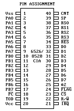
| 1 | Vss | Ground. |
| 2-9 | PA0-PA7 | Parallel
port A signals. Bi-directional parallel port. |
| 10-17 | PB0-PB7 | Parallel
port B signals. Bi-directional parallel port. |
| 18 | PC | Handshake output.
A low pulse is generated after a read or write on port B. |
| 19 | TOD | Time of day clock
input. Programmable 50Hz or 60Hz input. |
| 20 | Vcc | 5V DC input. |
| 21 | IRQ | Interrupt output
to microprocessor. |
| 22 | R/W | READ/WRITE input
from microprocessor's R/W output. |
| 23 | CS | Chip select input.
A low pulse will activate CIA. |
| 24 | FLAG | Negative-edge
sensitive interrupt input. Can be used as a handshake line for either
parallel port. |
| 25 | Phi2 | Phase 2 clock input.
|
| 26-33 | DB0-DB7 | Bi-directional data bus.
|
| 34 | RES | Low active reset input.
Initializes CIA. |
| 35-38 | RS0-RS3 | Register select
inputs. Used to select all internal registers for communications with the
parallel ports, time of day clock, and serial port (SP). |
| 39 | SP | Serial Port bi-directional
connection. An internal shift register converts microprocessor parallel data
into serial data, and visa-versa. |
| 40 | CNT | Count input. Internal
timers can count pulses applied to this input. It is used for frequency
dependent operations. |

