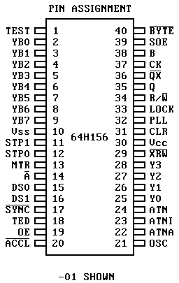
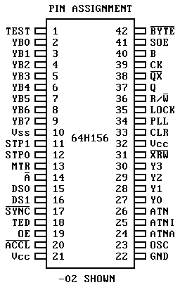
| 40 PIN | 42 PIN | DESC | FUNCTION |
|---|
| 1 | 1 | TEST | Input used in design verification. |
| 2-9 | 2-9 | YB0-YB7 | Data input/output lines for read/write operation. |
| 10 | 10 | Vss | Ground. |
| 11,12 | 11,12 | STP0,STP1 | Input to stepper driver. |
| 13 | 13 | MTR | Control line used to activate the stepper motor. |
| 14 | 14 | A | Write protect input. Indicates disk is write protected. |
| 15,16 | 15,16 | DS0,DS1 | Inputs used to produce the binary count for the frequency divide ratio. |
| 17 | 17 | SYNC | Sync output. |
| 18 | 18 | TED | A low input clears the BYTE line in 2 MHz mode. A high sets 1541 mode. |
| 19 | 19 | OE | Input to read/write block to set mode. 0 for Write, 1 for Read. |
| 20 | 20 | ACCL | Input select line for the CPU clock. 0 for 1541 - 1 MHz, 1 for 1571 - 2 MHz. |
| XX | 21,22 | | N/C |
| 21 | 23 | OSC | 16 MHz clock input. |
| 22 | 24 | ATNA | Attention acknowledge input. |
| 23 | 25 | ATNI | Attention line input from serial bus. |
| 24 | 26 | ATN | Attention data input from serial bus. |
| 25-28 | 27-30 | Y0-Y3 | Control output lines for the 4 phases of the stepper motor. |
| 29 | 31 | XRW | RAM write enable output. |
| 30 | 32 | Vcc | +5VDC. |
| 31 | 33 | CLR | High input when the read data is logical 1. |
| 32 | 34 | PLL | Input from the 20 pin gate array. Clock compensation. |
| 33 | 35 | LOCK | Indicates the PLL LOCK status. When logical 1, PLL is locked. When 0, the internal clock is used for sampling data. |
| 34 | 36 | R/W | R/W select input. |
| 35,36 | 37,38 | Q,Qx | Write pulse outputs. |
| 37 | 39 | CK | Clock select output - 1 or 2 MHz. |
| 38 | 40 | B | Write enable output. |
| 39 | 41 | SOE | Enable byte input. |
| 40 | 42 | BYTE | Data latched output. |